The STM32N6570-DK
Discovery Kit
A detailed tour of the hardware platform — from the physical board to the silicon architecture of the Neural-ART NPU — building the mental model needed to understand every deployment decision in this project.
The STM32N6570-DK Discovery Kit is a complete development and demonstration platform built around the STM32N657X0H3Q microcontroller — the first STMicroelectronics MCU to integrate a dedicated Neural Processing Unit (NPU) for on-device AI inference.
A Discovery Kit is not just a chip — it is a complete system that surrounds the microcontroller with all the peripherals needed to explore its capabilities immediately: a camera, a display, external memory, a debugger, and expansion connectors. This means we can run a full pose estimation pipeline — camera input, AI inference, display output — out of the box, without designing any custom hardware.
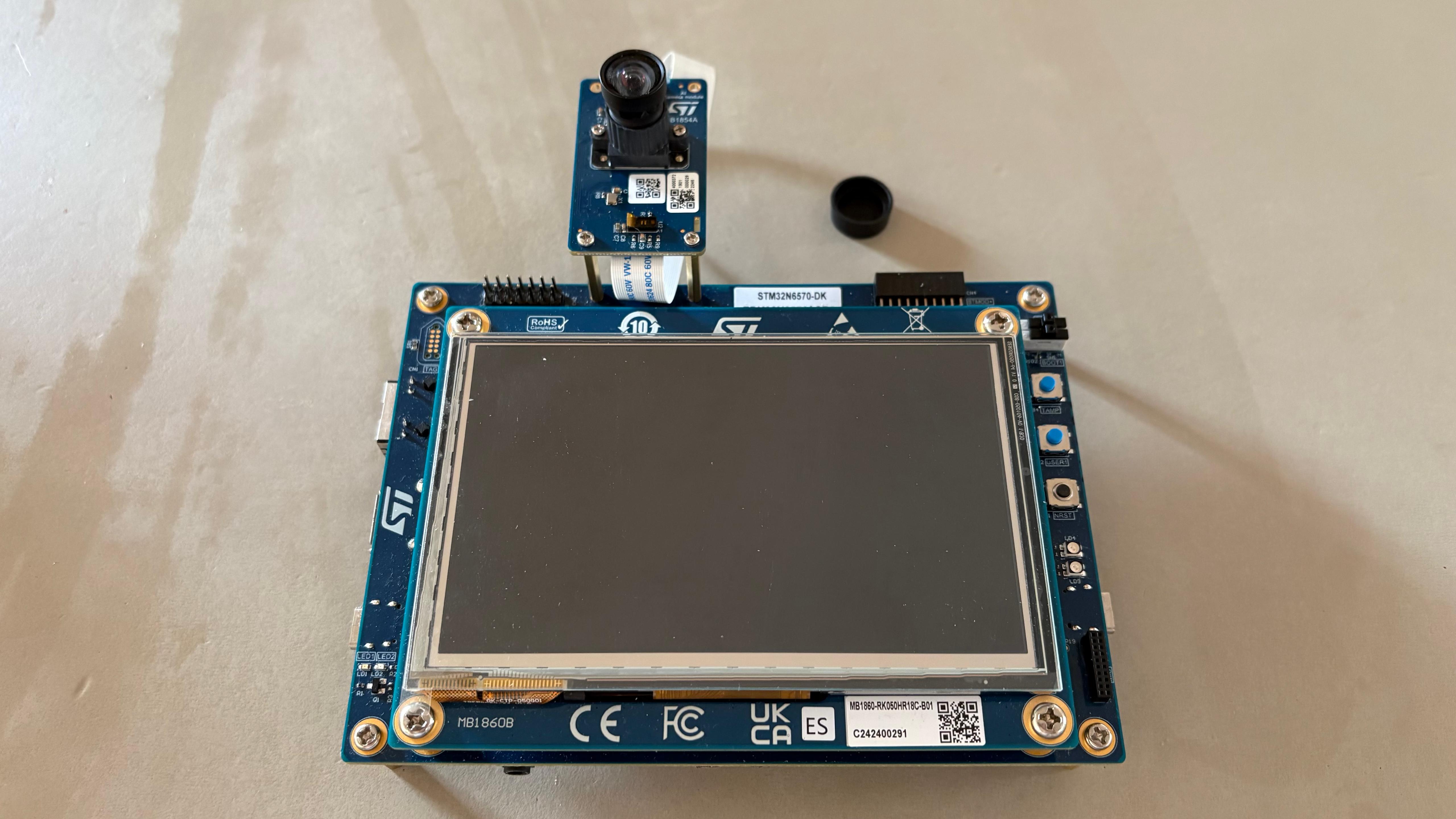
Understanding the board layout is important because many of the choices in our firmware — where data lives, how the camera feeds the NPU, why we need two XSPI interfaces — are direct consequences of the physical hardware. Let us walk through the key components.
| Component | Specification | Role in this project |
|---|---|---|
| STM32N657X0H3Q | Cortex-M55 @ 800 MHz, Neural-ART NPU, 4.2 MB SRAM | Runs all inference, camera control, display output |
| OctoFlash (XSPI2) | 1 Gbit = 128 MB, OPI mode, DTR transfer | Stores all model weights. Mapped at 0x70000000. Streamed to NPU during inference. |
| HexaRAM PSRAM (XSPI1) | 256 Mbit = 32 MB, HexaDecaSPI | Stores LCD framebuffers (800×480×2 bytes each). Too large for internal SRAM. |
| LCD Display | 5", 800×480, capacitive touch, RGB565/ARGB4444 | Shows camera preview (Layer 1) and skeleton overlay (Layer 2) simultaneously. |
| Camera connector | MIPI CSI-2, 2-lane | Receives frames from B-CAMS-IMX. Feeds DCMIPP for dual-pipe processing. |
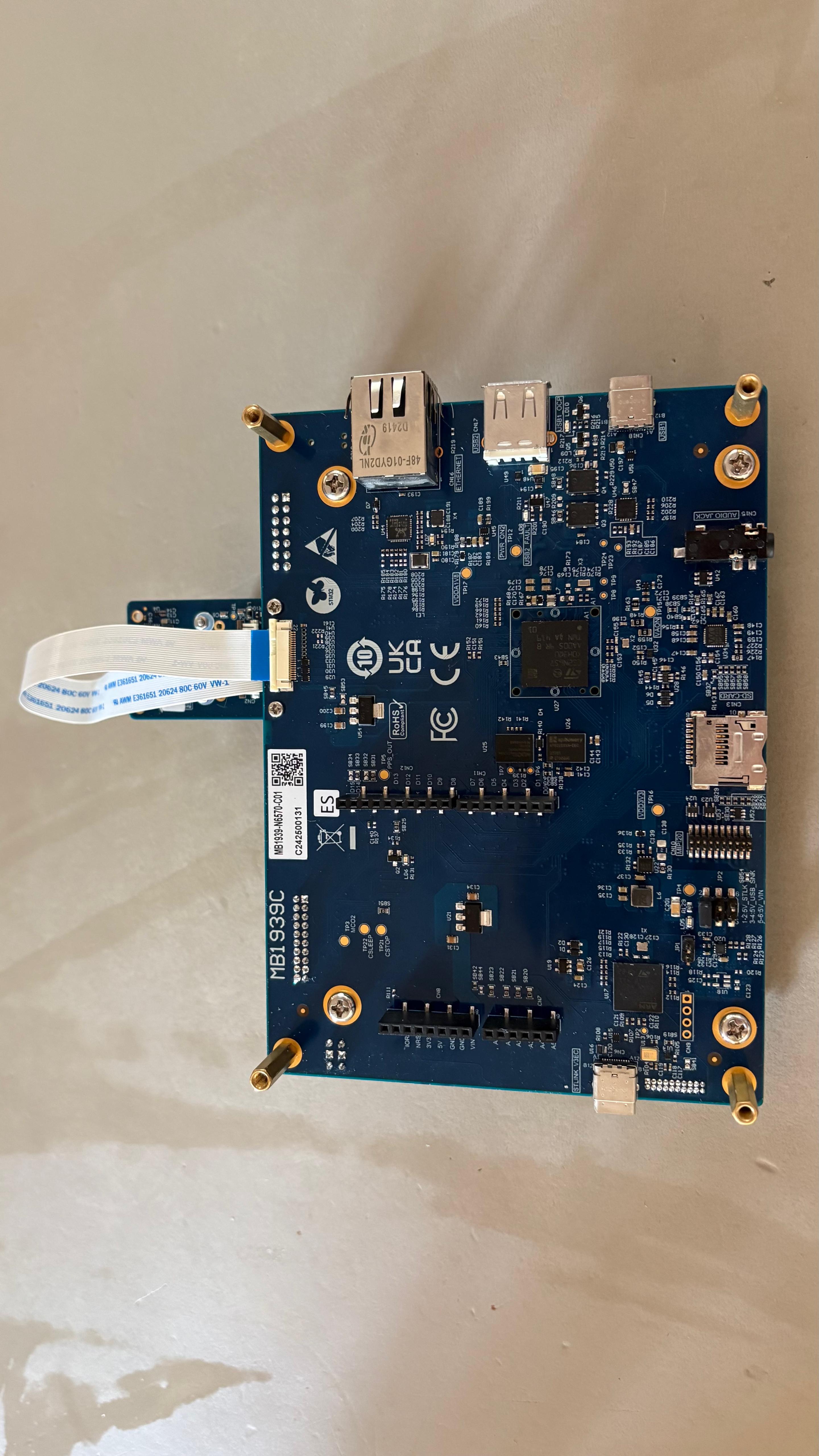
| STLINK-V3EC | Embedded debugger/programmer, USB Virtual COM | Used to flash firmware from STM32CubeIDE via USB. Also provides serial debug output. |
| Boot Switches | 2-position slide switches | RIGHT = flashing mode (needed before deployment). LEFT = run mode (needed to start inference). |
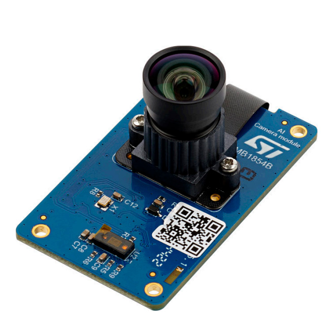
The B-CAMS-IMX is the camera daughter board included with the STM32N6570-DK. It carries a Sony IMX sensor and connects to the main board via the MIPI CSI-2 2-lane interface — the same interface used in smartphones for high-speed camera data transfer.
MIPI CSI-2 is a serial differential protocol that transmits pixel data at very high bandwidth with very few wires. Once the data arrives at the MCU, it is processed by the DCMIPP — a dedicated hardware block described in Section 2.6 — which handles format conversion, cropping, and routing to memory without CPU involvement.
The heart of the board is the STM32N657X0H3Q — a 264-ball VFBGA package integrating a complete system-on-chip. Let us zoom in from the package all the way to the silicon.
Three aspects of this chip are worth highlighting for our project:
The M55 is the first Cortex-M core with Helium (MVE) — a SIMD vector extension for signal processing and ML. It allows the CPU to process 16 INT8 values per clock cycle, which is critical for the SW epochs that fall back from the NPU.
Not a GPU. Not a general-purpose accelerator. A fixed-function hardware block designed specifically for CNN inference — with dedicated units for convolution, pooling, and activation. We will dissect it in detail in Section 2.5.
Dedicated video encoder and 2.5D graphics accelerator. Not used in this project but relevant context: this chip is designed for complete vision pipelines — capture, encode, analyse, display — all on a single MCU.
Understanding the memory hierarchy is not optional — it is the key to
understanding why the firmware is written the way it is. Every buffer placement
decision in main.c, every GCC section attribute in
network_data_params.c, and every cache invalidation call is a
direct consequence of this memory map.
| Region | Address | Size | Used for — MoveNet |
|---|---|---|---|
| npuRAM4 | 0x34270000 | 448 KB | nn_in: camera frame 192×192×3 = 110 KB. Input to NPU. |
| npuRAM5 | 0x342E0000 | 448 KB | nn_out: heatmaps 48×48×13 float32 = 120 KB. Output from NPU. |
| OctoFlash | 0x70380000 | 2.9 MB | Model weights. Read-only. Streamed to CONVACC via NPU AXI Cache. |
| PSRAM | 0x90000000 | ~1.5 MB | LCD background buffer (800×480×2) + foreground double-buffer. |
This is the most important section of the hardware chapter — and the one that directly explains our experimental results. The Neural-ART NPU is not a general-purpose processor. It is a fixed-function hardware accelerator designed with a very specific computation pattern in mind: the convolution operation that dominates CNN inference.
To understand why it is built this way, we need to understand what a convolution actually does at the hardware level.
A 2D convolution slides a small filter (e.g. 3×3 pixels) across an input feature map. At each position, it computes a dot product: multiply each filter weight by the corresponding input pixel and sum them all. For a single output pixel with 32 input channels: 3 × 3 × 32 = 288 multiply-accumulate (MAC) operations. For a full 192×192 feature map with 64 output channels: 192 × 192 × 288 × 64 ≈ 680 million MACs per layer.
This is a regular, predictable, data-parallel computation — the exact type that dedicated hardware handles far better than a general CPU. The CONVACC unit is built to execute thousands of these MACs per clock cycle by doing them in parallel.
- Conv2D (any kernel size)
- DepthwiseConv2D
- PointwiseConv (1×1)
- MaxPool, AveragePool
- ReLU, ReLU6, Sigmoid, Tanh
- BatchNorm, InstanceNorm
- Element-wise Add (residual)
- Fully Connected (as Conv)
- Softmax — required by attention in Transformers
- LayerNormalization — used in every Transformer block
- MatMul — Q·Kᵀ attention product
- Resize bilinear — used in MoveNet decoder
- Dequantize (INT8 → float32)
- Transpose, Reshape (some patterns)
- 1×1 conv when expressed as Dense
The DCMIPP (Digital Camera Memory Interface Pixel Pipeline) is a dedicated hardware block that sits between the MIPI CSI-2 camera interface and the MCU's memory. Its key feature for our project is the ability to run two simultaneous output pipes from a single camera input.
Now that we understand the NPU architecture, we can predict — and explain — the results we will measure in the Case Studies chapter. The key metric is the NPU offload rate: the fraction of computational epochs executed on the NPU hardware rather than falling back to the CPU.
ST Edge AI Core divides the model computation into a sequence of epochs — not training epochs, but execution blocks. Each epoch is assigned to either the NPU (EC epoch) or the CPU (SW epoch) depending on whether the NPU hardware supports that operation.
The pattern is clear and directly explained by the architecture:
Pure CNN backbone. Only 4 CPU epochs: 3× bilinear resize in the decoder and 1× dequantize output. The NPU was designed exactly for this.
CNN backbone (all NPU) + post-processing head (18 CPU epochs: reshape, softmax, transpose, slice). Heavy convolutions on NPU — real-time achieved.
96 CPU epochs across every Transformer block: Softmax (attention), LayerNorm, MatMul. These are the core operations — not post-processing. Real-time impossible.